 |
|
|
| CSP FBGA |
 |

| Product Overview |
| |
| This thin package solution has become available due to significant improvement in substrate and die thinning technology. |
| Package |
Total Thickness |
Package Profile |
Solder Ball Pitch |
| LFBGA |
1.20~1.70mm |
Low Profile |
Fine Solder Ball Pitch |
| TFBGA |
1.00~1.20mm |
Thin Profile |
Fine Solder Ball Pitch |
| VFBGA |
0.80~1.00mm |
Very Thin Profile |
Fine Solder Ball Pitch |
|
| * Small, thin and light package |
| * Flexible design |
| * Low cost and & time to market high volume production |
| * Competitive reliability performance (MSL3@260°C) |

|
| Application |
| |
| FBGA is commonly used in hand-held devices, like computer, communication, and consumer devices. Increasing demand for thin packages with high density performance make FBGA a highly competitive and reliable package solution to meet this growing demand. This package is highly recommended for Memory (SRAM, PSRAM, Flash, DRAM), Graph, ASIC, Digital and Analog products. |
|
| Features |
| |
 |
| |
| 3x3 mm to 21x21 mm body size available |
| Max 672 I/Os |
| 0.4/0.5/0.65/0.75/0.8/1.0 mm in ball pitch |
| Rigid and customized routing substrate design |
| High density interconnection |
| Full in-house design capability |
| Fine pitch wire bond capability |
| Low assembly cost |
| Self-alignment during re-flow |
| High speed performance |
| Lower profile (Package thickness) |
| RoHS/ Pb Free & Green Package process ready and available |
| Ease of thermal and electrical management |
| Ease of routing |
| JEDEC standard criteria |
|
|
| Reliability |
| |
| MSL3@260°C |
| Test Item |
Reference |
Condition/Duration |
| MSL Level 3 |
JEDEC 22-A103 |
30°C/60% RH, 192 hrs |
| TCT |
JEDEC 22-A104-B |
-65°C to 150°C, 500, 1000 cycles |
| HAST |
JEDEC 22-A118 |
130°C/85% RH, 33.5 PSI, 50/100, hrs |
| HTST |
JEDEC 22-A103-B |
150°C 500/1000 hrs |
| THT |
JEDEC 22-A101-B |
85°C/85%RH 500/1000 hrs |
|
|
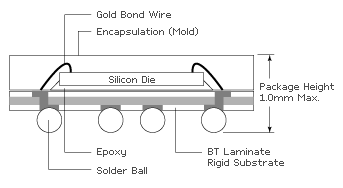
| Package Structure |
| |
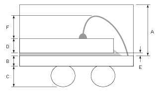 |
| ItemThickness (Total) |
Units |
LFBGA |
TFBGA |
VFBGA |
UFBGA |
| Total Thickness (Max) |
mm |
1.20~1.70 |
1.2 |
1 |
0.6 |
| Mold ThicknessPackage size (A) |
mm |
0.53~0.91 |
0.45~0.70 |
0.45~0.53 |
0.25 |
| Substrate thickness (B) |
mm |
0.21~0.56 |
0.21~0.36 |
0.21~0.26 |
0.13 |
| Solder ball height (C) |
mm |
0.16~0.46 |
0.16~0.40 |
0.07~0.23 |
0.16~0.22 |
| Wafer thickness (D) |
um |
125~200 |
125~200 |
100~150 |
75 |
| Max Epoxy (E) |
um |
50 |
50 |
38 |
25 |
| Max Loop height (F) |
um |
200 |
150 |
140 |
75 |
|
|
| Package Offering |
| |
| Package |
Body Size |
Lead Count |
| FBGA |
5x5 |
49, 65, 81 |
| FBGA |
6x6 |
92, 95 |
| FBGA |
6.2x6.2 |
81 |
| FBGA |
6x8 |
44, 48, 56 |
| FBGA |
7x7 |
64, 104 |
| FBGA |
8x8 |
120 |
| FBGA |
8.5x8.5 |
144 |
| FBGA |
8x10 |
56, 62, 64 |
| FBGA |
9x9 |
100, 156 |
| FBGA |
10x10 |
121, 128, 144 |
| FBGA |
11x11 |
182 |
| FBGA |
12x12 |
180, 193, 224, 240, 256, 257, 265, 300 |
| FBGA |
13x13 |
144, 176, 184, 200, 260, 280, 289, 293, 352 |
| FBGA |
14x14 |
349 |
| FBGA |
15x15 |
196, 217, 249, 256, 289, 324, 352, 384 |
| FBGA |
16x16 |
288, 569, 576 |
| FBGA |
17x17 |
256, 272, 360, 400 |
| FBGA |
19x19 |
324, 400 |
| FBGA |
21x21 |
400 |
| FBGA |
23x23 |
292 |
|
|
|
|